PCIe 8.0 Draft Unveiled: 1 TB/s Bandwidth, New Connectors, and a Path to 2028
The PCI-SIG has rolled out the first official draft of the PCIe 8.0 specification, setting ambitious performance targets that promise to reshape high-speed data transfer. This next-generation standard targets a blistering 256 GT/s data rate, delivering up to 1 TB/s of aggregate bandwidth in an x16 configuration. Alongside these speed gains, the spec introduces a novel connector design and achieves a critical 0.5V voltage milestone—all while maintaining backward compatibility with earlier PCIe generations. Final ratification is slated for 2028. Below, we break down the key details through a series of questions and answers.
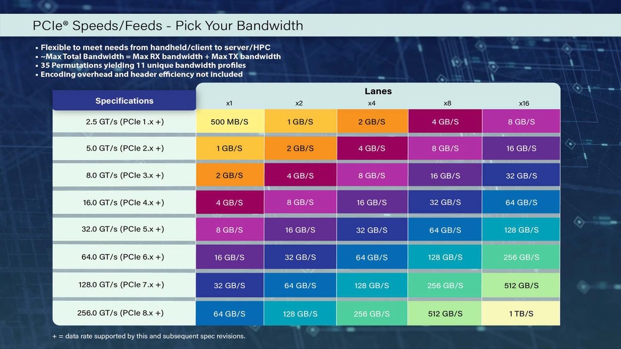
What is the headline performance target of PCIe 8.0?
PCIe 8.0 aims for a raw data transfer rate of 256 gigatransfers per second (GT/s) per lane. When combined in a typical x16 slot, this yields an aggregate bandwidth of roughly 1 terabyte per second (TB/s) in each direction. That's double the bandwidth of PCIe 7.0, which tops out at 128 GT/s. For context, a single PCIe 8.0 lane will handle up to 32 GB/s of bidirectional throughput, making it ideal for demanding workloads such as AI accelerators, high-performance networking, and next-generation storage arrays. The leap from 64 GT/s (PCIe 5.0) to 256 GT/s (PCIe 8.0) represents a fourfold increase over just two generations, underscoring the industry's relentless push for faster interconnects.
How does PCIe 8.0 achieve higher bandwidth while reducing power?
The PCIe 8.0 specification hits a key power-efficiency milestone by operating at just 0.5 volts—a reduction from PCIe 7.0's 0.8V. Lowering the voltage reduces dynamic power consumption per link, which is critical as signal integrity becomes harder to maintain at 256 GT/s. To compensate for the higher data rate, the standard uses advanced signal encoding and equalization techniques, such as PAM-4 (pulse amplitude modulation with 4 levels) and forward error correction. These methods allow reliable data transmission over copper traces of reasonable length without ballooning power budgets. Combined with the new connector design (see question 3), PCIe 8.0 effectively balances raw throughput with thermal and electrical constraints, enabling deployment in both server and consumer environments.
What new connector technology is being evaluated for PCIe 8.0?
PCI-SIG is assessing an updated connector for PCIe 8.0 that can handle the higher signal frequencies and tighter timing margins. While the full details remain under wraps, early documentation suggests a redesigned pinout and improved shielding to minimize crosstalk and insertion loss. One candidate includes a “mini” sideband connector for low‑latency control signals, decoupled from the main data lanes. The new connector also aims to maintain mechanical backward compatibility—so existing PCIe 7.0 or 6.0 devices could still physically plug into a PCIe 8.0 slot, albeit at slower speeds. This evolution ensures that the physical interface can support 256 GT/s without requiring exotic materials, keeping manufacturing costs in check for motherboard and add‑in‑card vendors.
Will PCIe 8.0 be backward compatible with older generations?
Yes, backward compatibility is a core requirement for PCIe 8.0. The specification maintains the same electrical and mechanical form factor as previous generations, meaning PCIe 8.0 slots can accept cards designed for PCIe 7.0, 6.0, 5.0, and earlier—with automatic negotiation down to the highest mutually supported speed. For example, a PCIe 4.0 graphics card inserted into a PCIe 8.0 slot will operate at PCIe 4.0 speeds (16 GT/s). This is critical for smooth upgrades and ecosystem stability. However, to achieve the full 256 GT/s, both the motherboard and the connected device must be PCIe 8.0 compliant. The PCI-SIG has also committed to using the same base specification framework, so software and firmware stacks developed for PCIe 7.0 will require only minor tweaks to support the new generation.

When can we expect final ratification of the PCIe 8.0 spec?
The PCI-SIG has set a target for final ratification of the PCIe 8.0 specification in 2028. The recently released version 0.3 draft is the first official step, followed by several revision cycles that incorporate feedback from member companies. Typically, PCI-SIG standards go through multiple draft versions (0.5, 0.7, 0.9) before reaching version 1.0. Given the technical challenges of 256 GT/s signaling and the new connector design, the timeline aligns with historical precedents: PCIe 7.0 took about four years from draft to ratification. Early adopters might see prototype hardware as early as 2026, but commercially available products will likely emerge in late 2028 or early 2029, coinciding with next‑generation CPU platforms.
What are the key milestones in the PCIe 8.0 development timeline?
PCIe 8.0’s roadmap includes several well‑defined milestones. The first major step was version 0.3 draft (announced in early 2025), which confirmed the 256 GT/s data rate and 0.5V voltage milestone. The next milestones are version 0.5 (refining electrical parameters and connector details), version 0.7 (integration of test methodologies), and version 0.9 (feature freeze). Final ratification as version 1.0 is expected by 2028. Simultaneously, the PCI-SIG will release compliance and interoperability test suites, allowing silicon vendors to validate their designs. In parallel, the connector evaluation work—led by a dedicated task group—will deliver a final mechanical specification by the version 0.7 stage. These phased releases help the industry prepare manufacturing tooling and driver support well ahead of finalization.
How does the 0.5V milestone benefit overall system design?
Reducing the operating voltage to 0.5V from 0.8V (PCIe 7.0) directly lowers the dynamic power per lane, which is crucial as lane counts multiply to achieve 1 TB/s. At the system level, this translates into lower heat generation and simplified power delivery on motherboards. For data centers, it means higher density of PCIe slots per rack without exceeding thermal limits. Additionally, lower voltage eases signal integrity design: smaller voltage swings reduce electromagnetic interference (EMI) and allow for longer trace lengths on dense PCBs. Designers can also use thinner, lower‑cost dielectric materials while still meeting eye‑opening requirements. Ultimately, the 0.5V milestone helps make PCIe 8.0 practical for deployment in both enterprise servers and consumer devices, where power‑efficiency is a top priority.
Related Articles
- 5 Valuable Lessons from Improving the tcpdump and dig Man Pages
- 10 Key Insights from Spark's New Risk Framework for the Sky Agent Network
- How to Apply Microsoft's May 2026 Patch Tuesday Updates: A Step-by-Step IT Admin Guide
- Organize Your Home Network with Static IP Addresses: A Step-by-Step Guide
- Bridging the Digital Divide: 8 Key Insights into IEEE’s Connecting the Unconnected Program
- 7 Essential Insights from Enhancing Man Pages for Dig and Tcpdump
- Smartphone Price Surge: OnePlus 15 and Nothing Phone Lead New Wave of Hikes in India
- Stop Zigbee Device Dropouts: The Simple Wi-Fi Channel Change That Costs Nothing